I wonder what the GPU market will be like in 2028...
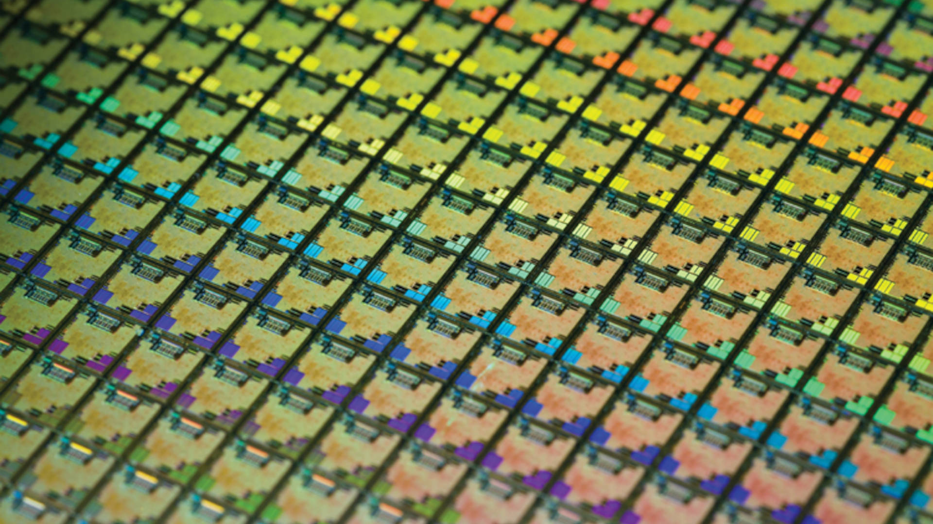
TSMC, the world’s biggest chipmaker, has just announced another process node which will almost certainly, amongst an undoubted slew of AI chips, be used to make some of our gaming GPUs and CPUs in the future. This next-gen process is ‘A14’, meaning 14 angstroms or 1.4 nanometres or really, really small.
This was announced yesterday at TSMC’s North America Technology Symposium, and the company says the process “is designed to drive AI transformation forward by delivering faster computing and greater power efficiency.”
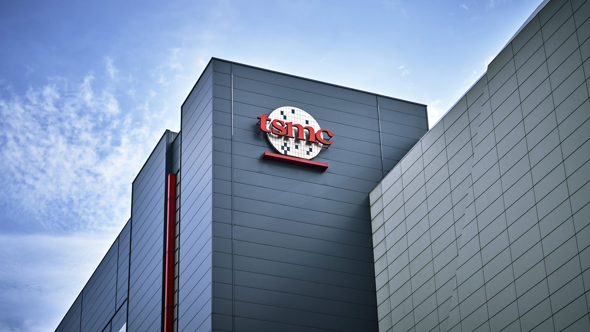
TSMC was already the world’s biggest chipmaker even before all this AI business started to really kick off, but ever since then, it’s a company name, alongside Nvidia, that’s on a ton of people’s lips. Naturally, then, talk of its upcoming process nodes will be of interest to many people, but we PC gamers can throw our hats into that pool of interested onlookers, too.
That’s because TSMC makes lots of the chips that end up in some of the best gaming CPUs and best graphics cards, whether from AMD, Nvidia, or even Intel. Currently, for instance, Nvidia RTX 50-series GPUs are made predominantly on TSMC’s 4 nm node, and the same goes for AMD’s Ryzen 9000-series processors. Intel’s Arrow Lake chips look to now be made exclusively by TSMC, too, ever since Intel killed its 20A process last year.
The newly announced A14 node is planned for 2028. Compared with its upcoming N2 process (set for later this year), TSMC says “A14 will offer up to 15% speed improvement at the same power, or up to 30% power reduction at the same speed, along with more than 20% increase in logic density.”
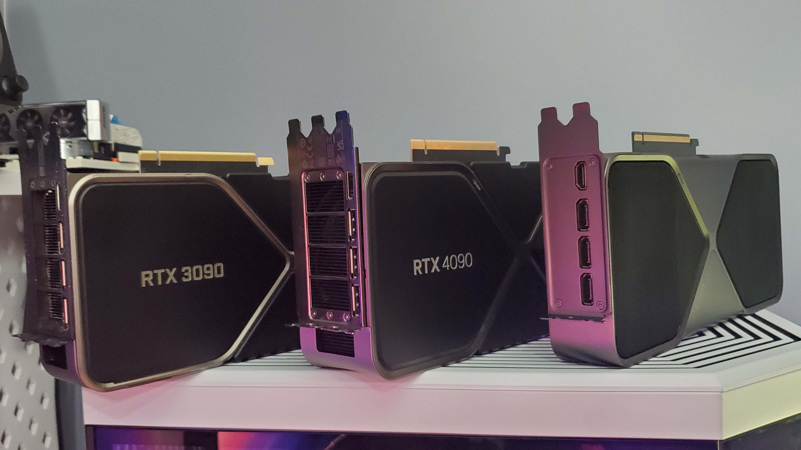
Although it’s a few years away, I can’t help but get a little excited about new processes. That’s primarily because we’ve seen with the RTX 50-series GPUS just how unexciting a new GPU generation can be if it doesn’t come off the back of a new process node (the RTX 50 series is on the same process as the RTX 40 series).
That being said, Nvidia doesn’t usually use bleeding-edge nodes for its GPUs, and we’ll be more likely to see AMD and Apple chips made using A14 to begin with.
A14 won’t have backside power delivery until 2029, either, according to our colleagues at Tom’s Hardware. Backside power delivery essentially moves power interconnects to the underside of the chip, reducing inference and the distance that power has to travel, thereby increasing efficiency and performance.
Best CPU for gaming: The top chips from Intel and AMD.
Best gaming motherboard: The right boards.
Best graphics card: Your perfect pixel-pusher awaits.
Best SSD for gaming: Get into the game ahead of the rest.
We expect to see backside power delivery (AKA ‘Super Power Rail’) from TSMC first with A16 in 2026. Intel’s ahead in this game, however, as its 18A process already has backside power delivery and is ready to go as of two months ago.
As for whether this A14 production will also make an appearance in the US, as well as from TSMC’s Taiwan fabs, it seems like it might. I’m basing this on the company’s recent earnings call, in which the company claimed that six fabs are planned in Arizona: “In that six fab, the 2-nanometer will be a major node, and that’s what I say, 30% will be there. As time goes by, after the 2-nanometer will be 1.4 and 1.0, that has not been discussed yet.”
This was in response to a question about what percentage of future leading nodes will come from the US vs from Taiwan, and to my ears it seems like TSMC is saying 1.4 and 1.0 will come from the US, but the percentage hasn’t been discussed yet.
Whatever the case, here’s to some healthy progress in process nodes across the board, whether from TSMC, Intel, or anyone else. Architectural and AI changes aside, raw performance increases are a direct result of transistor density, and we can all get behind that.