It's all about the defect density.
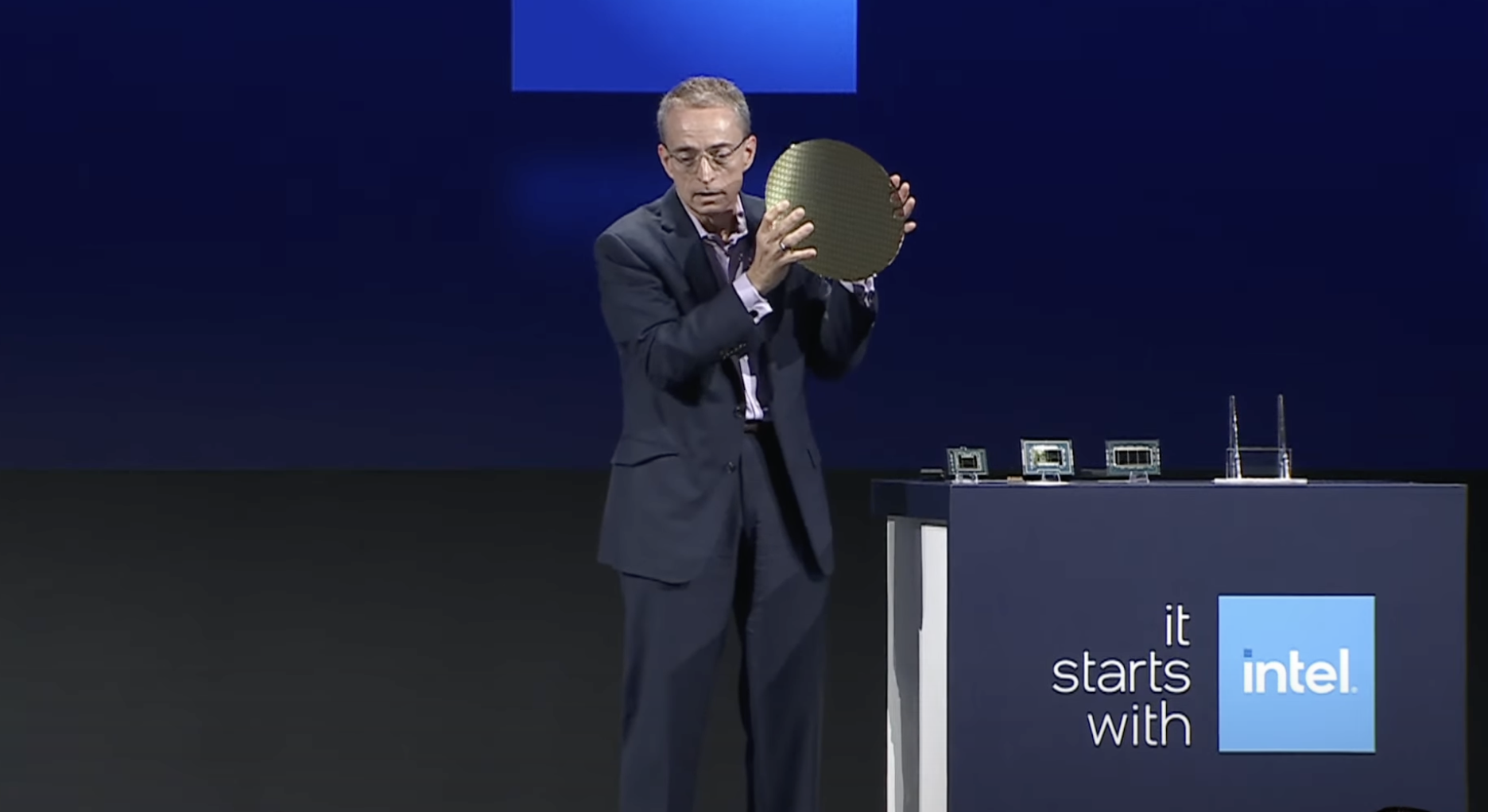
The $10 million he’s reportedly receiving in severance pay must soften the blow, but I can’t help but assume ex-Intel CEO Pat Gelsinger must surely feel the sting of Intel’s current situation and all reporting of its dire straits. The company is, after all, one he guided on a new journey towards increasing reliance on chip fabrication.
It therefore wouldn’t surprise me if Gelsinger’s recent comments on X (via Hot Hardware) regarding fabrication yields, while ostensibly about TSMC yields, were actually in part directed as a response to recent chatter about low Intel 18A yields.
Gelsinger says: “Speaking about yield as a % isn’t appropriate. Large die will have lower yield, smaller die – high yield percentage. Anyone using % yield as a metric for semiconductor health without defining die size, doesn’t understand semiconductor yield. Yields are represented as defect densities.”
This X post comes just a few days after Korean outlet Chosun Daily reported that Intel’s 18A process has just 10% yields, and just one day after it was picked up by the Western media at large—we also reported on it at PC Gamer but were sceptical about the claims because no sources were cited by Chosun Daily.
Whether coincidental or pointed, Gelsinger’s clarification is apt. “Yield” is how much of a wafer is usable for chips. But, as Gelsinger points out, the very same fabrication process can yield vastly different yields (sorry) depending on the size of the wafers being produced. Generally, the smaller the dies taken from the wafer the better the yield—ie, the lower the “defect density”.
The original 10% claims seemed to be related to Broadcom’s tests with the 18A node. But, as Tom’s Hardware points out, Broadcom is known for its use of gigantic chips. So one would expect lower yields for such customers. Plus, the 10% calculation only seems to factor in “perfect” dies, when in reality even many imperfect ones are usable as chips.
What really matters is that defect density number, which we’ve heard that Gelsinger had previously indicated to be below 0.4. Even if that did lead to a “low” yield for customers making giant dies, other similar process, for example from TSMC’s N2 process at a comparative time in its development, would also have such a “low” yield. The point is, from all we know—admittedly mostly based on Gelsinger’s own words—18A yields are perfectly fine compared to other new fabrication processes.
It can be easy to jump on the “sinking ship” bandwagon when it comes to Intel. There’s certainly plenty of reason to do so. But we can’t say that about 18A yet. It could end up being the one thing that keeps Intel afloat, given Gelsinger admitted he “bet the whole company on 18A”. And while I’m no gambling man, it still seems all bets are off.
Best CPU for gaming: Top chips from Intel and AMD.
Best gaming motherboard: The right boards.
Best graphics card: Your perfect pixel-pusher awaits.
Best SSD for gaming: Get into the game first.


