Except, of course, it won't really be 0.2 nm or anything even close to that.
Contrary to numerous pessimistic prognostications over recent years, including by Nvidia CEO Jensen Huang, Moore’s Law is very much alive and kicking. That’s the take-home according to a new roadmap from chip production research and engineering outfit IMEC. In fact, if IMEC’s roadmap is accurate, we already have a good idea how chip manufacturing is going to advance right through to 2039 and the 0.2 nm node.
Before we go any further, and as is always the case with Moore’s Law, the usual caveats apply. First, Moore’s Law isn’t a fundamental law of nature. It’s an observation of what’s happened in the past , projected into the future.
Specifically, it’s the observation (according to Intel), “that the number of transistors on a single chip doubles every two years at minimal costs.” In other words, you get chips twice as complex every two years for about the same price as before. Though the 2-year bit isn’t set in stone, so it’s not really a law per se, more a trend.
That latter stipulation regarding costs is the strongest argument against Moore’s Law’s extant status. Advanced chip manufacturing has gotten a lot more costly in recent years. Have you seen the price of GPUs?
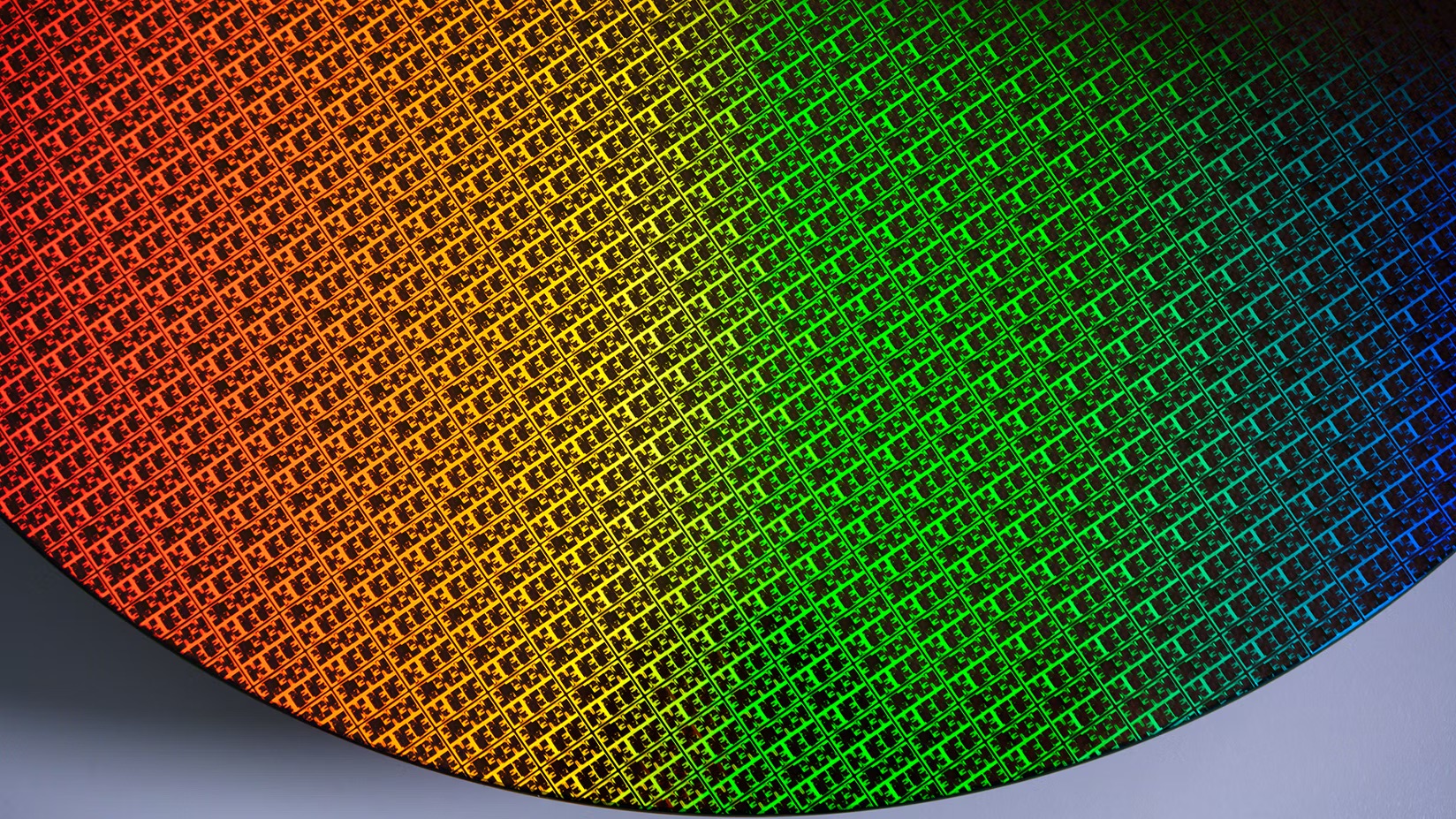
Anyway, the final proviso involves chip manufacturing nomenclature. Long story short, it’s become comprehensively detached from physical reality of late. In other words, the components inside a chip made on, say, 3 nm silicon, don’t actually measure 3 nm or anything close to that.
We’ll come back to the specifics in a bit, but first let’s take a look at what IMEC is predicting, courtesy of a new video on TechTechPotato. IMEC is an organisation that does much of the fundamental research around chip production, be that new materials, novel lithography techniques or next-gen transistor design.
Its output tends to propagate throughout the chip manufacturing industry, so it’s very well positioned to take a view on where chip tech is heading. And, actually, it’s looking pretty positive.
In terms of the basic process node, IMEC sees the industry moving from today’s cutting edge 3 nm technology, as currently offered by Taiwanese foundry TSMC, through to 14 A in 2027. The ‘A’ there stands for angstroms, a measure equal to 10 to the power −10 meters and the next rung down the ladder of tiny from nanometers or nm.
14 A is equivalent to 1.4 nm and IMEC expects it will be succeed by 10 A or 1 nm in 2029. IMEC sees that progression carrying on all the way through 2039, at which point we’ll be on a sub 2 A node, is something smaller than 0.2 nm.
Arguably, what’s more interesting than merely predicting that bi-annual cadence is the the technology that will enable it. On the lithography side of the equation, which involves the hugely complex machines that essentially print chips onto silicon wafers, IMEC predicts ever more advanced versions of today’s so-called extreme ultra-violet or EUV lithography will be good enough to hit that sub-0.2 nm target.
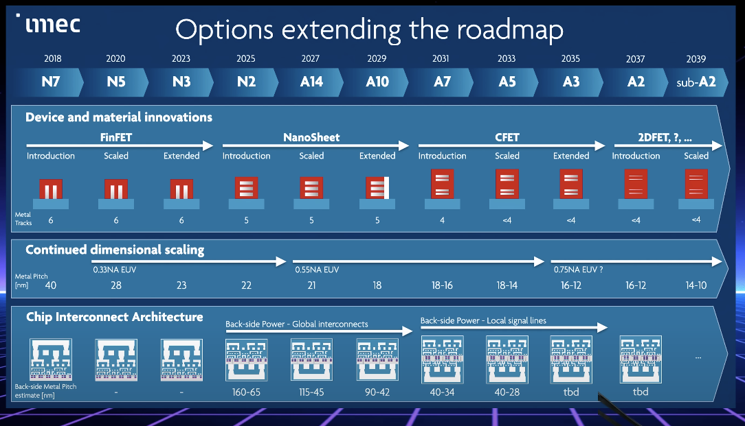
As for transistor tech, today’s FinFET transistors will be replaced by nanosheet transistors around 2027, with fork sheet transistors arriving in 2031 and then complimentary FETs after that, which are a a new kind of FET or Field Effect transistor that offer an immediate doubling of density.
Beyond that, IMEC expects some of the materials in chips will be 2D from 2037 onwards. In this context, 2D means sheets of material within the transistor measuring just one atom thick. It’s expected this will be done with some kind of material deposition. IMEC says one approach may be to “grow” 2D material on one wafer and then transfer it onto another.
Another enabling aspect will be the increased influence of interconnects for data and power on the underside of chip, something Intel calls “Backside Power” and is due to debut in Intel’s 18A chips including Panther lake at the end of this year. This reduces crosstalk between wires inside the chip, but it’s more complex to manufacture. IMEC sees that moving from today’s most basic backside interconnects, through global interconnects in 2 nm silicon and then backside interconnects with local signal lines around the 7 A node in 2031.
In terms of what all this means for the real sizes of the components inside chips, well, according to IMEC, in the most advanced 3 nm silicon, as currently offered by TSMC, the distance between the gate of one transistor to the next is actually 23 nm not 3 nm.
By the time we get to 14 A in 2027, that distance will be 21 nm and it will continue shrinking right through to 2039, when IMEC estimates it will measure between 14 nm and 10 nm.
So, yeah, you could argue that in reality we won’t have true 10 nm chips until roughly 2039. If that seems pretty disappointing, ultimately what matters is the ongoing progress, not what label you put on it. IMEC is predicting consistent node advances every two years through to 2039.
If that happens, chips in 2039 will be almost unimaginably complex. If you go back a similar amount of time, you get to 2011 and Intel’s Sandy Bridge CPUs built on 32 nm silicon.
An Intel Sandy Bridge Core i7 2700K chip had 1.1 billion transistors back in 2011. Today’s Intel Core Ultra 9 285K has just under 18 billion transistors. That would mean CPUs with around 300 billion transistors in 2039.
If you apply the same scaling to GPUs, which tend to have even larger transistor counts, we could be getting on for graphics chips with nearly 1.5 trillion transistors by the end of the next decade.
Anywho, that is of course a touch speculative. But the main take away here is that the complexity doubling bit of Moore’s Law appears to be alive and well. What will happen on the cost side of the equation, we’re rather less optimistic about.