Want to literally see inside the Switch 2's processor?
A new video from the ever effusive Geekerwan has broken down the details of the silicon at the heart of the Nintendo Switch 2. He picked up a bricked console motherboard for 1,000 Yuan (approx. $140) from a Chinese eBay analogue, Xianyu, and has absolutely gone to town on the chip.
Like, above and beyond.
I absolutely recommend you watch the video, because as well as being incredibly detailed on the extent they went to in order to get the full details of the chip—including cutting it down the middle with a very thin ion beam in order to measure a cross-section to ascertain the process node—he’s super-engaging and always enthusiastic about what he’d covering. It’s a joy, honestly.
Anyways, the main takeaway is that yes, this is the Nvidia T239 chip that was widely rumoured to be the chip powering the new Nintendo handheld, and you can see from the metal layer inscription that this was a processor taped out in 2021. Geekerwan notes that this four-year gap is a very long time between tape out and release, and likely hints at a Switch 2 that was supposed to be released a while back and was postponed for whatever reason.
It’s Nintendo; the reason could be anything.
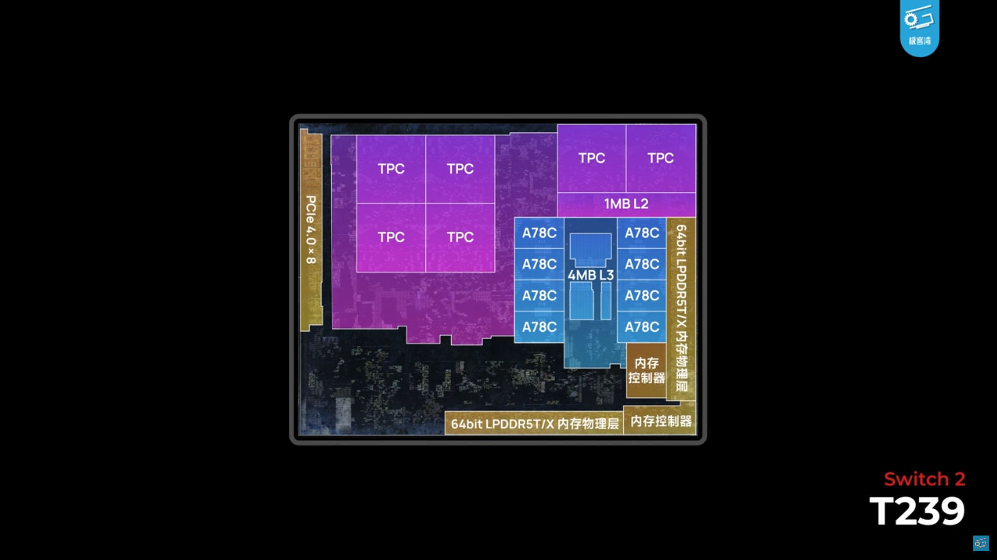
Because it’s an already broken chip—they tried powering it on, but got nowhere—there was nothing stopping them from ripping the Nvidia chip open to see what was going on under the logo’d heatspreader. Lapping the top meant they could get a great die shot, highlighting that while this does indeed house Ampere-generation Nvidia hardware, “this Ampere is not the other Ampere.”
There are definite differences between an RTX 30-series die and the layout of the GPU component in the T239 chip. Geekerwan notes that the SM design actually looks far closer to the layout of an Ada SM than an Ampere one, which could suggest that there are some elements shared between the GPU generations on this chip.
There are 12 SMs on this board, with 128 CUDA cores in each, for a total of 1536 cores. That’s what the rumours had already said, so that’s not a surprise here.
Another thing which seems to straddle two generations is the process node itself. Theoretically, it’s a Samsung 8N node, but their examination suggests this is a production process that shares features of both Samsung’s 10 nm and 8 nm nodes. This is, however, a custom process, so that does make sense.
With the GPU parts strangely wrapped around it, there is the CPU segment. This is made up of eight Arm A78C cores, each with 256 kB L2 cache, with a shared 4 MB of L3 in the middle.
As well as ripping the wrapping layers off this silicon present, Geekerwan has also made an attempt at trying to dial into the potential performance of the Switch 2’s core. With a similarly Ampere-based GPU, the GA107 of the RTX 2050 laptop chip is the closest match, though that comes with a far higher TGP and memory and core clocks.
In order to try and get a bead on gaming performance, they hobbled their RTX 2050 laptop as best they could to match the rumoured handheld frequency of the Switch 2—421 MHz—and halved the memory clock. To get that low, they needed to employ internal tools to bring the target TGP and frequencies right down.
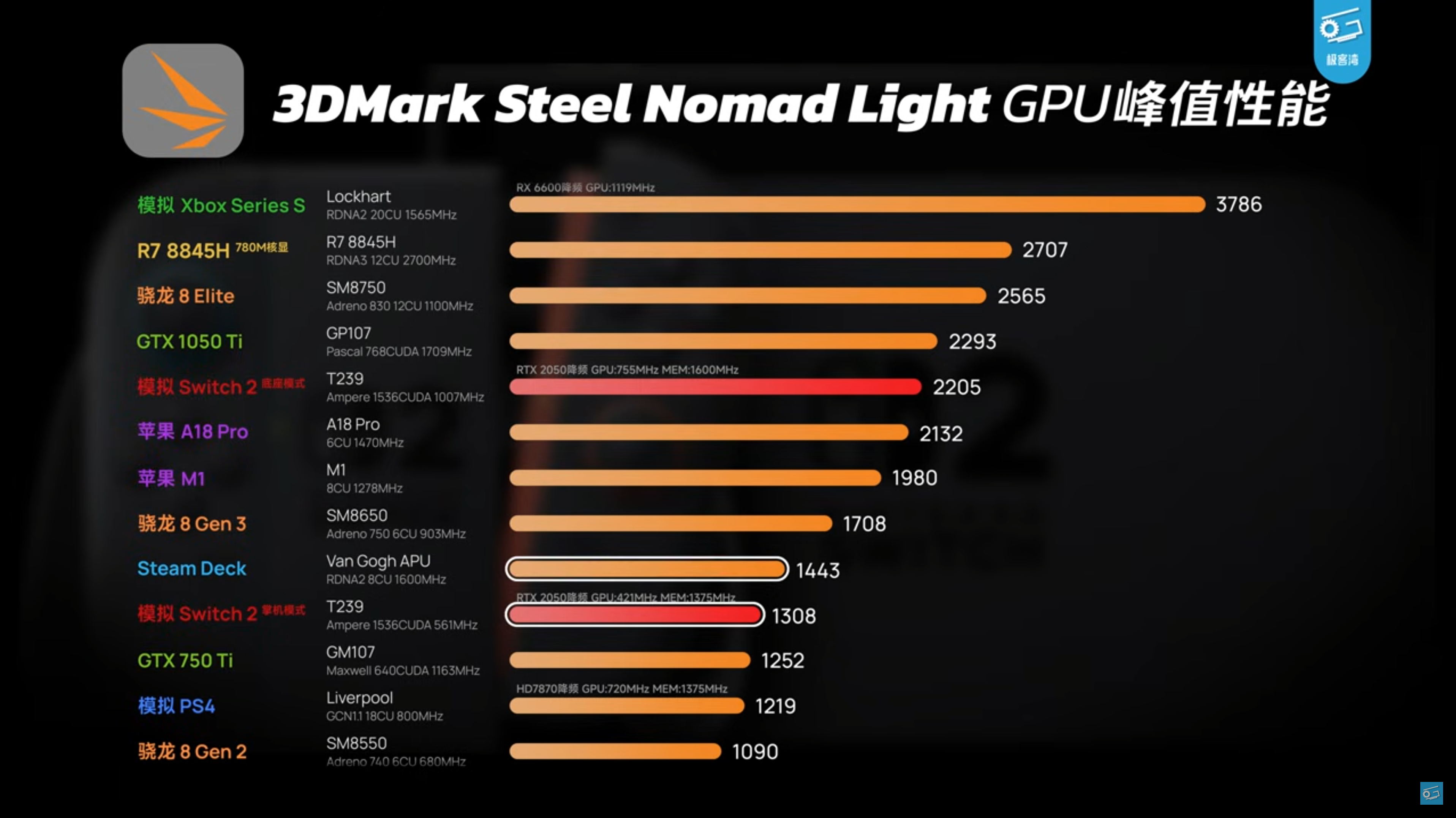
Taking 3DMark Steel Nomad Light as their GPU test, you can see that in handheld mode, the Switch 2 actually has a similar level of performance as the Steam Deck, with the docked mode simulating 53% higher performance than Valve’s classic handheld.
Though it’s worth noting that even in docked mode, it can’t touch the Radeon 780M, which powers most of the rest of the handheld gaming PCs on the market.
One thing they do note, however, is that while there is a significant difference between the original Switch chip and the theoretical performance of the new one, it’s not the 10x that Nvidia has been touting. At least not without DLSS, and maybe even Frame Gen. Remember that we said there were similarities between the Ampere GPU in the T239 and the Ada design?
Best handheld gaming PC: What’s the best travel buddy?
Steam Deck OLED review: Our verdict on Valve’s handheld.
Best Steam Deck accessories: Get decked out.
Steam Deck battery life: What’s the real battery life?
Geekerwan then goes on to show a simulated Cyberpunk 2077 run at the expected DLSS levels that a Switch 2 version, in both handheld and docked mode, might deliver. And, well, it’s not bad, especially when you think it’ll be on a relatively wee screen. He did turn on path tracing, too, but the less said about that the better.
The same goes for Monster Hunter Wilds where he says, “even if you run 720p, low-definition, super-performance DLSS in dock mode, it becomes a shitty wilderness.” Though Black Myth Wukong doesn’t look bad, and the latest CoD also runs pretty well on this simulated hardware.
As you might expect, it’s the CPU component that is way behind the GPU part. The Arm cores run at 1.1 GHz, and in a Geekbench 6 analysis, that puts the simulated performance 140% behind the Steam Deck APU’s single-core performance and 52% behind on multi-core metrics.
It’s a really interesting breakdown of the Switch 2’s potential performance, and a great look at the actual silicon, too. And, again, I say go watch the video, this guy’s great.