7 GHz-plus computing here we come...?
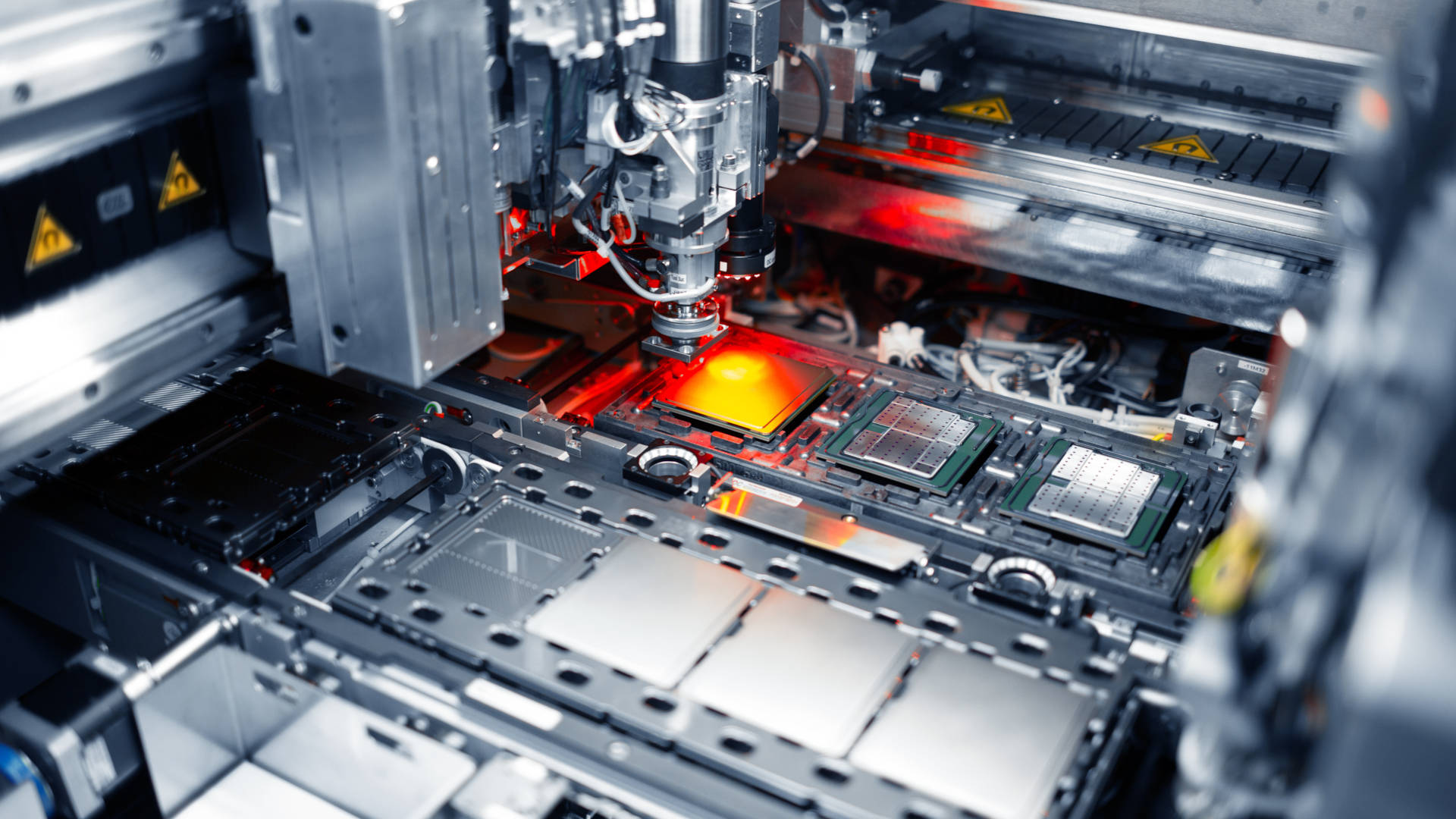
Silicon has dominated the chip industry as its foundational material since, well, forever. But now researchers at Peking University claim to have cooked up a novel approach to integrating transistors using, yup, you didn’t guess it, bismuth. The result (via Interesting Engineering) is said to be 40% more speed in return for a 10% lower power compared to the latest commercial chip tech from Intel and TSMC.
The Peking team outlines the new technology in a snappily-title research paper, in Nature, “Low-power 2D gate-all-around logics via epitaxial monolithic 3D integration.”
But what exactly is bismuth, I hear you cry? Well, the Peking team has used bismuth in both the semiconductor and high-dielectric oxide. It’s a post-transitional metal, which also applies to lead, gallium, indium and tin, among others. Silicon, by contrast, is a metalloid and a semiconductor in a wide array of contexts, while bismuth is only a semiconductor when deposited in sufficiently thin layers. So, now you know.
Incidentally, all this is going on at the same time as Huawei is testing a new extreme ultra-violet (EUV) lithography machine that’s said to be competitive with the best that ASML can produce, the latter being the company that makes the machines used by TSMC, Intel et al, and which will supposedly go into production later this year.
To get back to the Nature paper and quote the killer line, “here we report a wafer-scale multi-layer-stacked single-crystalline 2D GAA configuration achieved with low-temperature monolithic three-dimensional integration, in which high-mobility 2D semiconductor Bi2O2Se was epitaxially integrated by high-K layered native-oxide dielectric Bi2SeO5 with an atomically smooth interface, enabling a high electron mobility of 280 cm2 V−1 s−1 and a near-ideal subthreshold swing of 62 mV dec−1.”
Yeah, 62 mV dec−1, suck it up Intel and TSMC! Actually, no, I have no idea what that means, either. Notably and somewhat more comprehensibly, the team claims a 30 nm gate length. If that sounds a lot bigger than today’s supposed 3 nm technology from, say, TSMC, the reality is that the likes of “3 nm” are more marketing terms than reflective of the physical realities of current technology.
By way of example, TSMC’s N3E node as used in the latest Apple chips has gate pitch of at minimum 45 nm and a metal pitch of 23 nm. Intel’s 18A node is said to have a 30-36 nm metal pitch. Either way, nowhere near 3 nm.
The claimed upshot includes the aforementioned 1.4x operating speeds at 90% power consumption versus cutting edge commercial silicon nodes. Given that Intel and TSMC nodes are hardly identical, it’s not clear how that is calculated. However, if you take 5 GHz as a rough yardstick for top-end current chip speeds, excluding a few relative edge cases, you’d be looking at a 7 GHz processor, which is getting on some.
As a result, the Peking team claims they have, “the fastest, most efficient transistor ever.” Whether they actually do or not is another matter. But this research, along with the Huawei lithography machine, certainly feeds into a broader narrative of the Chinese building momentum in chip tech.
Will they close the gap? It very much seems a question of when, not if. Of course, it’s a separate question as to whether this bismuth-based chip tech will be part of that. There have been numerous attempts over the years to replace silicon as the material of choice for chips. None have succeeded. Yet.
Best CPU for gaming: Top chips from Intel and AMD.
Best gaming motherboard: The right boards.
Best graphics card: Your perfect pixel-pusher awaits.
Best SSD for gaming: Get into the game first.