N2 is quite a bit more efficient but only a little more dense than N3.
Everyone’s favorite uber chip foundry TSMC has been dishing the deets on its next-gen node, known as N2 (via Tom’s Hardware). And the take home is that its both more efficient and more dense than TSMC’s current N3 tech, but perhaps not dramatically so.
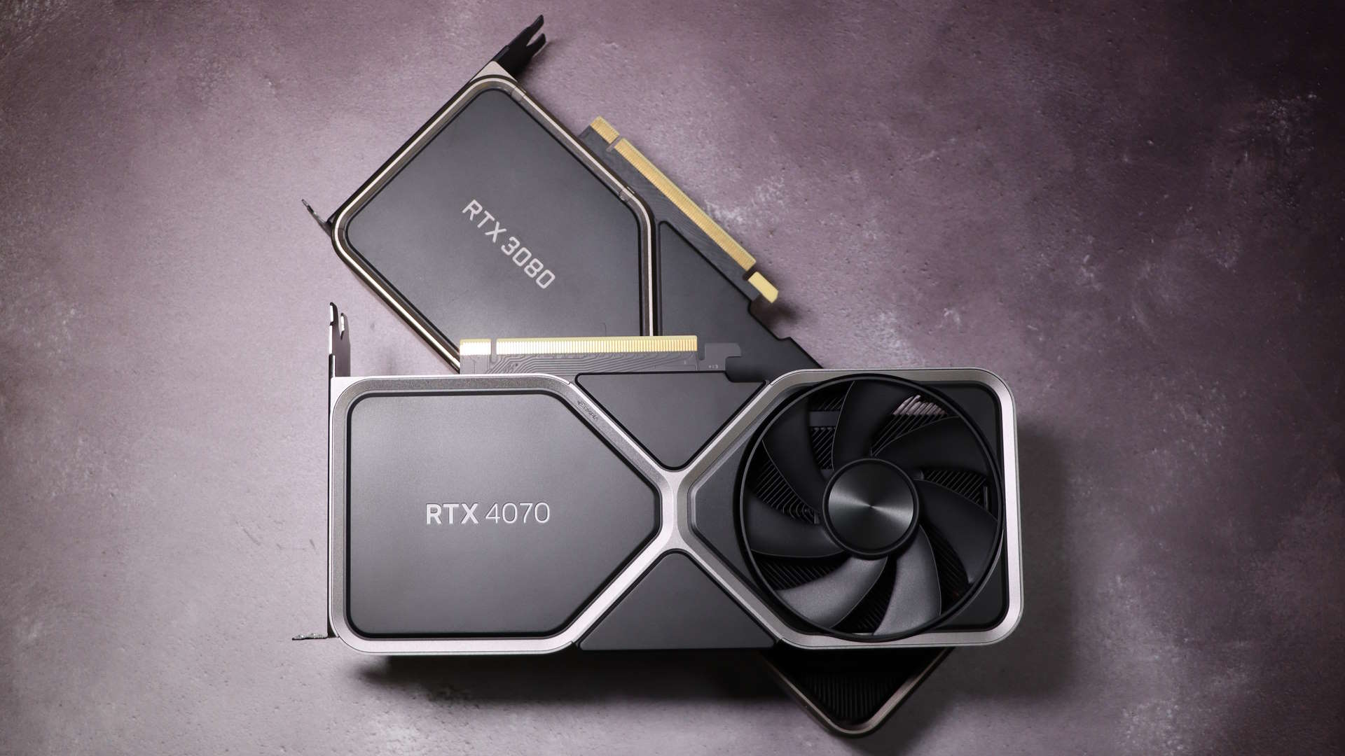
Still, the good news is that still gives us at least two generations of GPUs on new silicon nodes to look forward to. That’s because current GPUs are all based on derivations on TSMC’s N5 silicon.
So, you would expect both AMD and Nvidia (and Intel if they’re still in the GPU game) to move to TSMC’s current cutting edge chip manufacturing process, N3, at some point, followed by N2. All of which means there’s decent scope for progress on the pure process side of things for some time to come.
Indeed, prevailing rumors suggest both of AMD and Nvidia’s next-gen graphics chips, including the likes of the mooted Nvidia RTX 5090 and its Blackwell siblings, will remain on N5-derived silicon (likely to be branded N4). That means N2 provides an upgrade path several years down the road.
Anywho, what of the specifics of N2? In terms of density, TSMC is only claiming 1.15x progress over N3, or just 15%. That means TSMC will be able to pack in 15% more transistors per unit of chip area compared to N3.
That’s a pretty modest step for a new node. However, it’s worth bearing in mind two things.
First, given that’s the improvement over N3, the overall increase in density versus today’s N5/4 based GPUs will be pretty substantial.
What’s more, TSMC is claiming improved SRAM density for N2. SRAM density scaling has hit a bit of a wall of late, with TSMC claiming no improvements in that regard for N3 over N5. However, N2 is claimed to achieve 38Mb/mm^2 to N3’s 33.55 Mb/mm^2, which is a decent step.
Long story short, SRAM takes up a fair bit of space on most chips, so the inability to shrink SRAM cells was becoming an increasing problem. N2 is therefore looking like an important node even with modest overall transistor shrinkage.
Best CPU for gaming: The top chips from Intel and AMD.
Best gaming motherboard: The right boards.
Best graphics card: Your perfect pixel-pusher awaits.
Best SSD for gaming: Get into the game ahead of the rest.
Efficiency is the other part of the puzzle and here TSMC is claiming 25% to 30% progress over N3. Broadly, that efficiency can either be used to enable the same performance for less energy usage, or more performance at the same power budget.
As for timing, the first retail chips based on the N2 node are expected in the second half of next year and will most likely be seen in an Apple product, perhaps branded Apple M5.
As for chips for PCs, well, as above next year’s AMD and Nvidia GPUs are actually thought to still be N5-derived. Unless both outfits skip N3, therefore, you would normally expect N3-based GPUs in 2027 with N2 chips in 2029, which in turn would be the best you could buy through to early 2031.
As you can see, then, TSMC’s N2 tech provides a roadmap for new GPUs and indeed CPUs for many years to come. And that’s very good news indeed.


