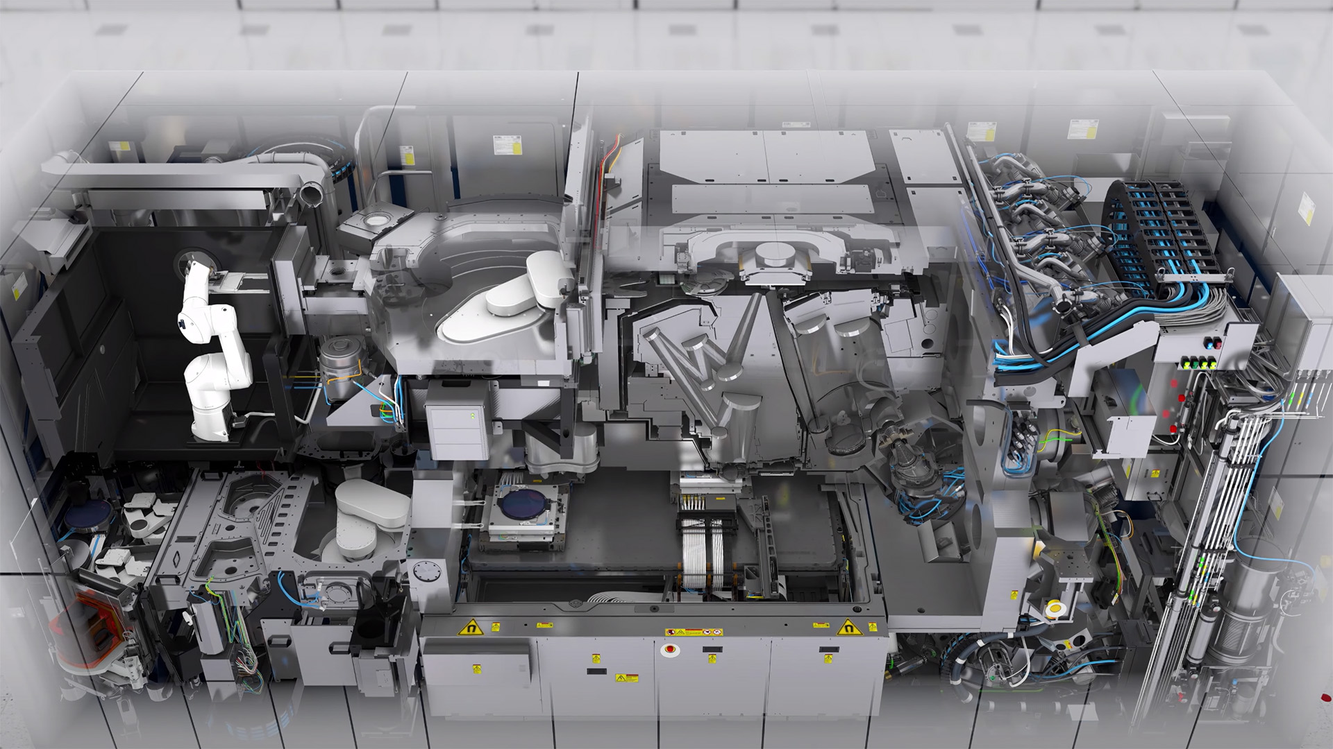
CEO Huang explains the fundamentals of EUV lithography. And that's way more interesting than it sounds.
Nvidia’s CEO Jensen Huang just summed up how the next-generation of chip manufacturing will work, and the video clip makes for great watching if you’re in any way interested in the incredibly complex and expensive process.
The segment from Huang’s GTC keynote above explains how machines from a company called ASML will create the next-generation of computer chips. ASML provides lithographic machines to every major chip manufacturer, including TSMC, used by Nvidia, AMD and Intel; and Intel’s own foundry. ASML’s latest and greatest are built for what’s known as EUV, or extreme ultraviolet lithography, a highly complex way of printing ever-shrinking circuits onto silicon chips.
It’s easy to sum up EUV and the entire modern lithographic process as “magic” or “miraculous”, as Huang himself does, but it’s just incredibly complicated. EUV technology has been decades in the making, and felt at one point like it might never arrive. In essence, however, EUV tries to simplify the already incredibly time-consuming and complex DUV (deep ultraviolet) lithographic process used today.
EUV is the key to shrinking transistors down to smaller sizes required for more advanced process nodes, and thus more advanced CPUs and GPUs with more circuitry squished inside them. TSMC rolled EUV out with its N7+ node, and uses EUV for more and more layers with its N5 and N3 process nodes, while Intel will use EUV from its Intel 4 node onwards.
In the video there’s an impressively detailed diagram of an ASML EUV machine—a massive device that costs somewhere in the ballpark of $250 million.
And Huang is making such a fuss of ASML and EUV during his keynote speech because Nvidia is announcing a new tool, cuLitho, that uses GPU acceleration on its graphics cards to speed up the process of designing the masks used in lithography by some 40x.
Yeah, Nvidia’s paying TSMC to make its GPUs only to sell them right back to it. That’s a commercial play if ever I saw one.


